The pace of modern technological development - from microelectronics to catalysts, to coatings - is driven by
fundamental breakthroughs in fabricating novel nano-structured materials. Such materials often promise unique or
enhanced physical characteristics, such as strong magnetisation or unusual reactivity. These characteristics will
derive from, but can also be compromised by, subtle, atomic-scale structural variations. In each case,
nano-resolved characterization is essential and full understanding of a material demands multiple state-of-the-art
experimental probes. The probes used in my research include beams of electrons, atoms, ions, and photons, as
well as physical devices such as the tip of an atomic force microscope. Each probe has its advantages and its
limitations and the best studies of nanostructured material combine the results from several probes in order to develop
a complete description.
A selection of my recent projects is given below. The uppermost projects derive from my time in Glasgow, whilst
some of those below are based on collaboration with colleagues in Cambridge, where more information can be found.
|
|
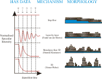
 Even in the absence of spatial resolution, the technique of helium atom scattering (HAS) is of
tremendous utility in observating thin film growth processes, adsorption dynamics and surface
structure. I have been involved in a variety of HAS studies, for example showing that current
state-of-the-art calculations cannot predict accurately the ground state adsorption site of atomic
hydrogen on a copper (111) substrate - in many senses, one of the simplest possible adsorption
systems. More details of this and other studies can be found from my Publications and the Cambridge Surface Physics group webpages,
where I also wrote a brief overview of the HAS technique and its
instrumentation.
Publications: 8,9,11-15.
|


