PhD Opportunities 2018/19
All PhD positions have been filled for the current academic year but further opportunities may be available with my colleagues.
Studentship opportunities are administered by the Glasgow Materials & Condensed Matter Physics group,
a very active research group with a strong international reputation well and excellent funding through the funding councils,
research councils and industry. Students of the group receive training in a number of high-performance electron microscopy and
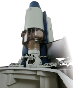
surface analytical techniques, using the world class equipment of the Kelvin Nanocharacterisation
Centre, and are also enrolled in the Graduate School of the Scottish Universities Physics Alliance.
Doctoral students are liable for tuition fees in addition to subsistence costs and most students finance their studies via competitive scholarships,
some of which are outlined here.
The Scottish Universities Physics Alliance (SUPA) has a particularly prestigious scheme, with an application closing
date around the end of January: more details can be found here.
Full details of the application process are available from the Graduate School
of the College of Science and Engineering, although I would strongly encourage all potential applicants to make
contact with me in advance of submitting a formal application.
A selection of previously-advertised projects is listed below.
Pulsed laser deposition of advanced oxide materials

As part of a major new investment, the Kelvin Nanocharacterisation Centre is installing a pulsed laser deposition
system for the fabrication of a variety of thin film devices and coatings. The pulsed laser deposition technique is
almost ideal for depositing the complex, multi-component materials now being proposed by theorists as being essential
to the next generation of microelectronic devices. However, even atomic-scale defects, dislocations, impurities and
strain can impair performance and the optimal fabrication conditions are simply unknown in most cases. This project
will assist in the commissioning of the new deposition system and will characterise the nanometric structure of a
variety of multi-component oxide materials for technological applications. A combination of electron diffraction,
scanned probe microscopies and transmission electron microscopy will be used to characterise the samples and the
student will gain highly-transferable skills in materials deposition and high resolution characterisation. The project
will suit students with an interest in instrumentation and chemical physics and has the opportunity for collaboration
with a number of national and international partners.
Development of dynamic, pump-probe electron microscopy techniques

Transmission electron microscopy (TEM) allows the direct imaging and characterisation of materials on length scales
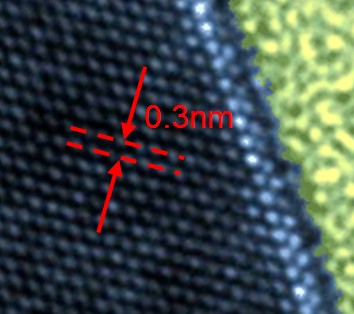
ranging from microns to nanometres, and with the advent of aberration corrected instruments, sub-Angstrom analysis is
becoming routine. As a consequence, the TEM technique has become essential to nanotechnology, materials science and
biosciences, providing both the structural and chemical information to understand samples ranging from microprocessor
circuits to biological cells. In recent years, the phenomenal capabilites of TEM have been extended to the time domain
and there is increasing interest in capturing dynamic events such as crystallisation, chemical reactions and
microelectronic device operation in real time. This project will develop protocols for time-resolved TEM and is
expected to be of high impact across several disciplines. It will use the world-leading facilities of the Kelvin
Nanocharacterisation Centre, which are soon to be complemented by a multi-million pound installation of a new
aberration corrected microscope, and may extend to use of the national synchrotron facility, Diamond, for ultra-fast
nanoanalysis. The project will suit able students with an interest in instrumentation, interfacing and
nanocharacterisation.
Development and characterisation of Resistive Random Access Memory

Resistive random access memory (Re-RAM) is a candidate 'storage-class' memory technology, capable of replacing both
conventional random access memory (RAM) and hard disk drives (HDDs). It offers in a single, simple device the
non-volatility and write-endurance of HDDs with the rapid access times of conventional RAM. Furthermore, Re-RAM has the
potential for stacked, 3-dimensional architectures and intrinsic multi-state functionality, which together could
truly revolutionise data storage densities. At its simplest, a Re-RAM element comprises two electrodes sandwiching an
active component. Structural or chemical bistability in the active component causes large, hysteretic resistance
changes that can be used to distinguish between at least two memory states. Unfortunately, little is known about the
atomic-scale processes that underpin the bistability, which is a major barrier to commercialisation. This project will
use state-of-the-art materials deposition and characterisation facilities to investigate the operation of ReRAM
materials. The student will fabricate and study a number of prototype ReRAM devices, gaining world-class training in
transmission electron microscopy, focused ion beam patterning, etc. It is a tremendously exciting opportunity in an
extremely high impact area. |


